PCB Specifications
Features | Capability | Notes | Patterns |
Layer count | 1,2,4,6 layers | The number of copper layers in the board. |
|
Controlled ImpedanceMaterial | 4/6 layer, default layer stack-up
| Controlled Impedance PCB Layer Stackup siampcb Impedance Calculator |
|
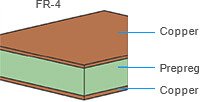
Material | FR-4 | FR-4 Standard Tg 130-140/ Tg 155 |
|
Dielectric constant | 4.5(double-side PCB)
| 7628 structure 4.6 2313 structure 4.05 2116 structure 4.25 |
|
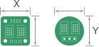
Max. Dimension | 400x500mm | The maximum dimension siampcb can accept |
|
Dimension Tolerance | ±0.2mm | ±0.2mm for CNC routing, and ±0.4mm for V-scoring |
|
Board Thickness | 0.4/0.6/0.8/1.0/1.2/1.6/2.0mm | The thickness of finished board. |
|
Thickness Tolerance (Thickness≥1.0mm) | ± 10% | e.g. For the 1.6mm board thickness, the finished board thickness ranges from 1.44mm(T-1.6×10%) to 1.76mm(T+1.6×10%) |
|
Thickness Tolerance (Thickness<1.0mm) | ± 0.1mm | e.g. For the 0.8mm board thickness, the finished board thickness ranges from 0.7mm(T-0.1) to 0.9mm(T+0.1). |
|
Finished Outer Layer Copper | 1 oz/2 oz (35um/75um) | Finished copper weight of outer layer is 1oz or 2oz. |
|
Finished Inner Layer Copper | 0.5 oz (17um) | Finished copper weight of inner layer is 0.5oz only. |
|
Drill/Hole Size
Features | Capability | Notes | Patterns |
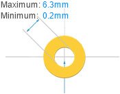
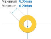
Drill Hole Size (Mechanical) | 0.20mm- 6.30mm
| Min. drill size is 0.20mm. Max. drill size is 6.30mm. |
|
Drill Hole Size Tolerance | +0.13/-0.08mm | e.g. for the 0.6mm hole size, the finished hole size between 0.52mm to 0.73mm is acceptable. |
|
Blind/Buried Vias | Don’t support | Currently we don't support Blind/Buried Vias, only make through holes. |
|
Min. Via hole size | 0.2mm | For Single&Double Layer PCB, the minimum via hole size is 0.3mm;For Multi Layer PCB, the minimum via hole size is 0.2mm |
|
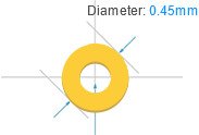
Min. Via diameter | 0.45mm | For Single&Double Layer PCB, the minimum Via diameter is 0.6mm;For Multi Layer PCB, the minimum via diameter is 0.45mm. |
|
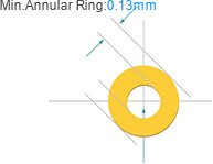
PTH hole Size | 0.20mm - 6.35mm | The annular ring size will be enlarged to 0.15mm in production. |
|
Pad Size | 0.70mm- 6.35mm | The pad hole size will be enlarged 0.15mm in production. |
|
Min. Non-plated holes | 0.50mm | The minimum NPTH dimension is 0.50mm, Please add the NPTH in the mechanical layer or keep out layer. |
|
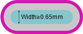
Min. Plated Slots | 0.65mm | The minimum plated slot width is 0.65mm, which is drawn with a pad. |
|
Min. Non-Plated Slots | 1.0mm | The minimum Non-Plated Slot Width is 1.0mm, please draw the slot outline in the mechanical layer(GML or GKO) |
|
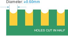
Min. Castellated Holes | 0.60mm | The minimum diameter of castellated holes is 0.60mm. |
|
Hole size Tolerance (Plated) | +0.13mm/-0.08mm | e.g. for the 1.00mm Plated hole, the finished hole size between 0.92mm to 1.13mm is acceptable. |
|
Hole size Tolerance (Non-Plated) | ±0.2mm | e.g. for the 1.00mm Non-Plated hole, the finished hole size between 0.80mm to 1.20mm is acceptable. |
|
Rectangle Hole/Slot | Don’t support | We don't make rectangle hole/slot,the rectangle hole/slot will be made as round or oval hole/slot by default. |
|
Minimum clearance
Features | Capabilities | Patterns |
Hole to hole clearance(Different nets) | 0.5mm |
|
Via to Via clearance(Same nets) | 0.254mm |
|
Pad to Pad clearance(Pad without hole, Different nets) | 0.127mm |
|
Pad to Pad clearance(Pad with hole, Different nets) | 0.5mm |
|
Via to Track | 0.254mm |
|
PTH to Track | 0.33mm |
|
NPTH to Track | 0.254mm |
|
Pad to Track | 0.2mm |
|
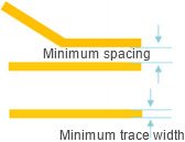
Minimum trace width and spacing
Copper weight | Min. Trace width | Min. Spacing | Patterns |
H/HOZ (Inner layer) | 5mil (0.127mm) | 5mil (0.127mm) |
|
1oz (Outer layer) | 1/2 layers: 5mil (0.127mm) 4/6 layers: 3.5mil(0.09mm) | 1/2 layers: 5mil (0.127mm) 4/6 layers: 3.5mil(0.09mm) |
|
2oz (Outer layer) | 8mil (0.2mm) | 8mil (0.2mm) |
|
BGA
Layer count | Min. BGA Pad Dimensions | Min. Distance Between BGA | Patterns |
1/2 layers | 0.4 mm | 0.127mm |
|
4/6 layers | 0.25 mm | 0.127mm |
|
Solder Mask
Features | Capabilities | Notes | Patterns |
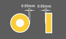
Solder mask opening/ expansion | 0.05mm | The solder mask should have a minimum of a 0.05 mm "growth/mask opening" around the pad to allow for any mis-registration. |
|
Solder bridge | 0.2mm(green) 0.254mm(other colors) | To have solder mask bridge, the spacing between copper pads edge must be 0.2mm (8mils) or more. |
|
Solder mask color | green, red, yellow, blue, white, and black. | We use LPI (Liquid Photo Imageable) solder mask. It is the most common type of mask used today. |
|
Solder mask dielectric constant | 3.8 |
|
|
Solder mask thickness | 10-15UM |
|
|
Legend
Features | Capabilities | Notes | Patterns |
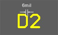
Minimum Line Width | 6 mil (0.153mm) | Characters width less than 6mil(0.153mm) will be unidentifiable. |
|
Minimum text height | 32 mil (0.8mm) | Characters height less than 32mil(0.8mm) will be unidentifiable. |
|
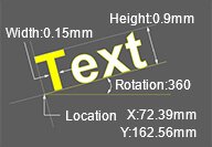
Character width to height ratio | 1:6 | The preferred ratio of width to height is 1:6. |
|
Pad To Silkscreen | 0.15mm | The Minimum Distance Between Pad and Silkscreen is 0.15mm. |
|
Features | Capabilities | Notes | Patterns |
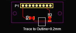
Trace to Outline | 0.2mm | Ships as individual board(Rounting):Trace to Outline≥0.2mm |
|
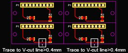
Trace to V-cut line | 0.4mm | Ship as panel with V-scoring: Trace to V-cut line≥0.4mm |
|
Panelization
Features | Capabilities | Notes | Patterns |
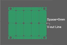
Panelization without space | 0mm | The space between boards is 0mm. |
|
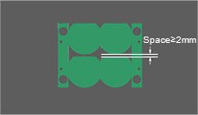
Panelization with space | 2mm | Make sure the space between boards should be ≥2mm,otherwise it will be hard to process for rounding. |
|
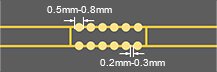
Panelized Round board | ≥20mmx20mm | The single round board size should be≥20mmx20mm. Panelize with stamp holes and add tooling strips on four board edges |
|
Panelized castellated holes board | Panelize with stamp holes and add tooling strips on four board edges | The distance between castellated hole and board corner should be larger than 4mm. Recommended diameter of stamp hole is 0.5mm-0.8mm; Recommended distance between the two stamp holes is 0.2-0.3mm |
|
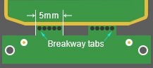
Min. Width of Breakaway Tab | 4mm | The minimum width of breakaway tab is 4mm. For breakaway with mouse-bites, the minimum width is 5mm. |
|
Min. Edge Rails | 4mm | If choosing panel by JLCPCB, we will add 5mm edge rails on both sides by default. |
|
รายการ | ความสามารถในการผลิต | รายละเอียด |
| ชั้นลายวงจร (Layer) | 1 - 6 ชั้น | ไม่สามารถทำ Blind/Buried Vias ได้ (Via ซ่อนไว้ด้านใน) |
| วัสดุ | FR-4 | |
| ขนาด PCB | 400 x 500 mm | *สำหรับ PCB 1 - 2 ชั้น ขนาดใหญ่สุด 400 x 500 mm. *สำหรับ PCB หลายชั้น ขนาดใหญ่สุด 300 x 300 mm. |
| ขนาด PCB (ความคลาดเคลื่อน) | ±0.2 mm | ความคลาดเคลื่อนจากเครื่องจักรในการผลิต CNC V-scoring |
| สีสารเคลือบ PCB | เขียว, ขาว, น้ำเงิน, ดำ, แดง, เหลือง | |
| ความหนา PCB | 0.4/0.6/0.8/1.0/1.2/1.6/2.0 mm | |
| ความหนา PCB (ความเลาดเคลื่อน) | ±0.1mm - ±10% | |
| ความหนาของทองแดง | 1 oz - 2 oz | |
| ความหนาของทองแดงชั้นใน | 0.5 oz | |
ระยะต่ำสุด เส้น/ระยะห่างเส้น | 3.5mil (0.089 mm) | *สำหรับ PCB 1 - 2 ชั้น ขนาดต่ำสุด ระยะห่างเส้น/ความกว้างเส้น 5 mil. *สำหรับ PCB หลายชั้น ขนาดต่ำสุด ระยะห่างเส้น/ความกว้างเส้น 3.5mil. |
ขนาดต่ำสุด รู (Via) | 0.2mm | *สำหรับ PCB 1 - 2 ชั้น ขนาดเล็กสุด ขนาดรู 0.3mm. (Via) *สำหรับ PCB หลายชั้น ขนาดเล็กสุด ขนาดรู 0.2mm. (Via) |
ขนาดต่ำสุด เส้นผ่านูนย์กลาง | 0.45mm | *สำหรับ PCB 1 - 2 ชั้น ขนาดเล็กสุด ขนาดเส้นผ่านูนย์กลาง 0.6mm. (Via) *สำหรับ PCB หลายชั้น ขนาดเล็กสุด ขนาดเส้นผ่านูนย์กลาง 0.45mm. (Via) |
ระยะต่ำสุด รู(Via) กับ เส้น | 5mil (0.127 mm) | ระยะห่างระหว่างรู Via กับ เส้นลายวงจร 5mil |
ขนาดรูเจาะ Drill Hole Size | 0.2-6.3mm | ขนาดเล็กสุด 0.2mm / ขนาดใหญ่สุด 6.3mm. |
| ความคลาดเคลื่อนรูเจาะ | ±0.08mm | |
ขนาดเล็กสุด เส้นรอบวง | 3mil (0.076 mm) | |
ขนาดเล็กสุด ตัวอักษร | 6mil / 32mil (0.152 / 0.813 mm) | ความหนา 6mil / ความสูง 32mil |
ระยะห่างระหว่างเส้นกับขอบPCB | 0.2mm | *การตัดPCBในงานแบบชิ้น (Routing):ตัดงานเป็นชิ้นๆ ระยะห่างเส้นกับขอบงาน ≥0.2mm; *การตัดPCBในแบบงานเป็นชุดV-scoring:V-cut ระยะห่างเส้นกับเส้นV-cut ≥0.4mm |
ระยะห่างของงานเป็นชุด | 2mm | ควรมีระยะห่างระหว่างบอร์ด ≥2mm ไม่อย่างนั้นจะยากต่อการผลิต จากการ Routing (CNC) |
ขนาดกว้างต่ำสุด. ขอบราง PCB | 3mm | |
| Copper Hatching with Pads | Hatch | สามารถทำได้ตามที่ลูกค้าออกแบบมาได้เลย (Copper Regions,Track Arcs) |
| Slot Drawing with Pads | Outline | หากมีหลายรูที่ไม่ชุบ (NPTH) โปรดรายละเอียดให้ด้วย |
| Protel/dxp Solder Layer | Solder Layer | Paste Layer ในProtel/dxp ไม่ใช่ Solder Layer (ข้อควรระวัง) |
| Protel/dxp Outline Layer | Keepout Layer/Mechanical Layer | ออกแบบขอบงานควรเลือกเป็น Keepout Layer/Mechanical Layer สำหรับเส้นขอบ,Routing , V-cut ควรใส่รายละเอียดมาให้ด้วย |
ขนาด. เส้นผ่านศูนย์รูเจาะเป็นครึ่งวงกลม Min. Half Hole Diameter | 0.6mm | การเจาะรูแบบพิเศษครึ่งวงกลม เส้นผ่าศูนย์กลางรูควรมากกว่า 0.6 mm |
Soldermask Bridge/ Blind and buried vias | Soldermask Bridge/Blind and buriedvias ไม่สามารถทำได้ | |
| โปรแกรมที่เราสามารถใช้ได้ | Altium Designer/Protel99/Proteus/ Gerber File | เป็นโปรแกรมที่ทางเราสามารถ Support ได้ ไฟล์ที่ใช้ในการผลิตจะเป็น Gerber File |